

TSMC has released a promotional video on YouTube, showing off all the hard work it's put into the construction and operation of its brand new facility, TSMC Arizona. Situated in the open desert just outside of the state capital, Phoenix, the chipmaking facility is shown to be utterly vast, from its huge, solar panel-fronted footprint to its 2001: A Space Odyssey-like interiors.
"What we're building is a city", says the narration, over a soaring soundtrack. Yep, it sure looks like one alright.
"On site we have 3,000 engineers, technicians, support folks, people from all over the US, from South America, from Asia," says Rose Castanares, the president of TSMC Arizona. "So many people coming together for a particular mission."
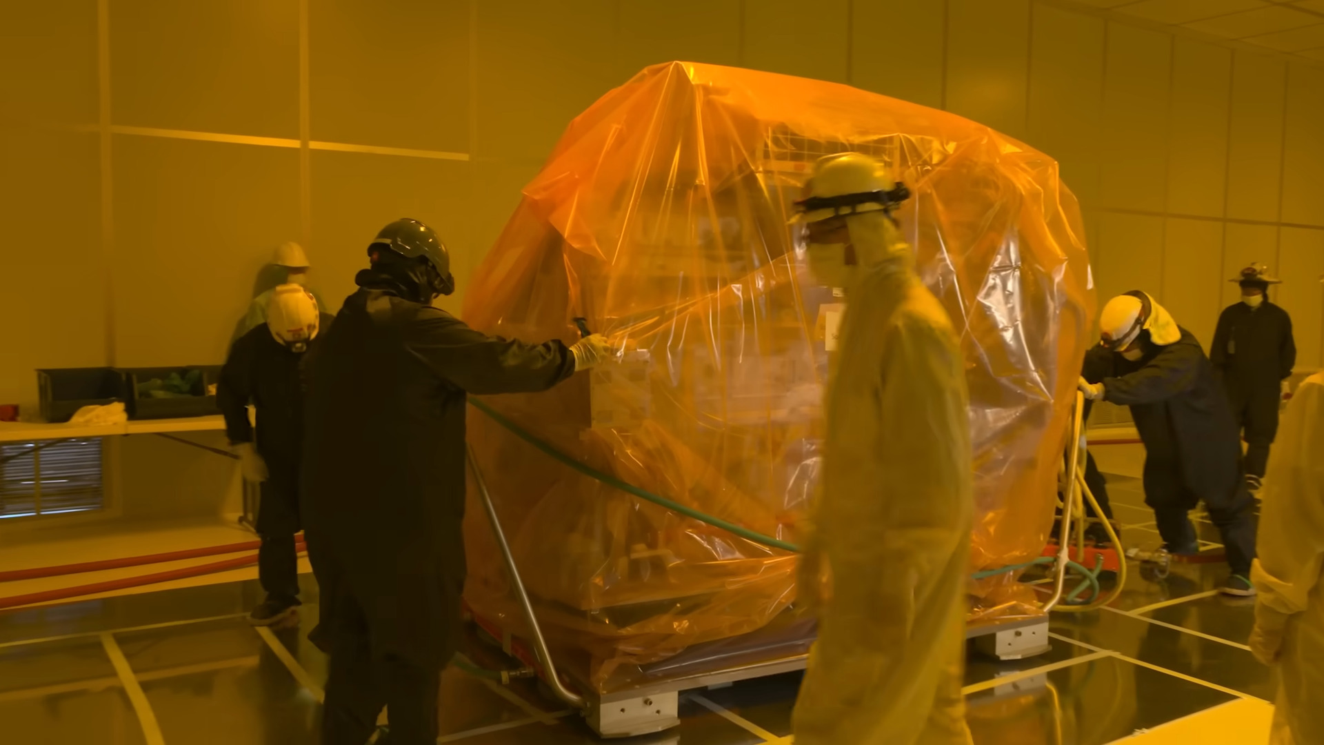
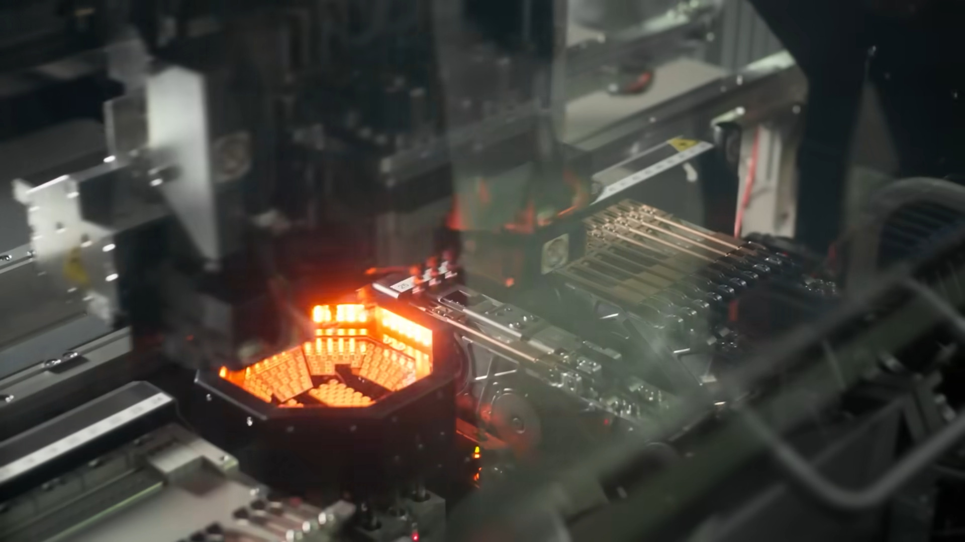
And that mission, of course, is to build some of the world's most advanced chips on US soil. Delving into the labyrinthine interiors, we're shown towering, yellow-lit rooms of phenomenal scale, along with the arrival of advanced lithography equipment, vital for the production of TSMC's newest processes.
There's something slightly comforting about such high-value pieces of equipment being wheeled in on hand-pushed carts, looking more like well-wrapped sofas in a house move than machines capable of pumping out the most advanced silicon on the planet. Although, closer inspection doesn't appear to show any wheels underneath. Instead, a sequence of hoses seems to be floating the equipment on its way towards its final destination. Where do I get one of those for my next move?
"It's a remarkable milestone" says TSMC Arizona vice president Y.H. Wu, as the first of these machines glides through its doors. "We bring [chip] manufacturing back to the USA."
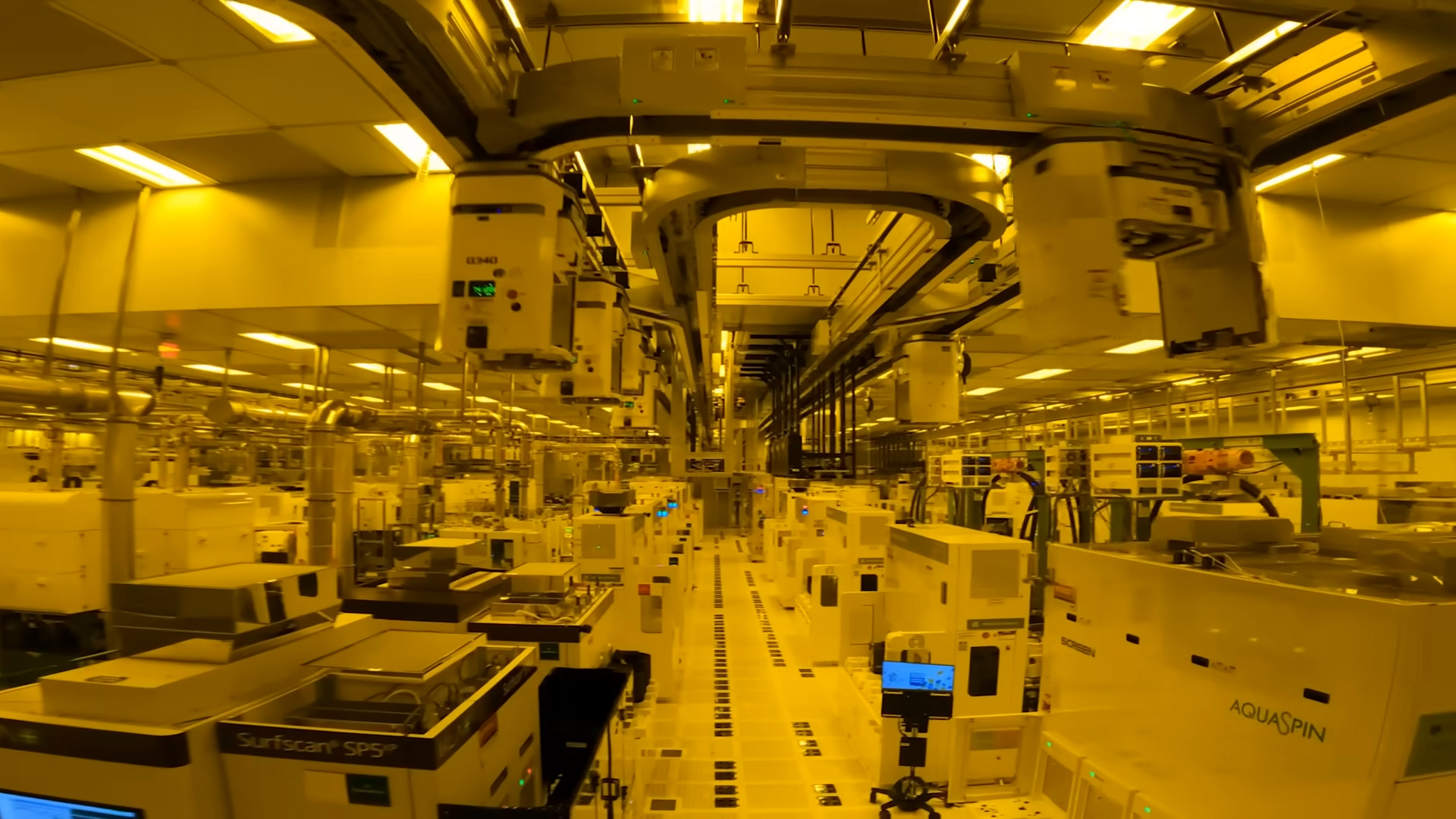
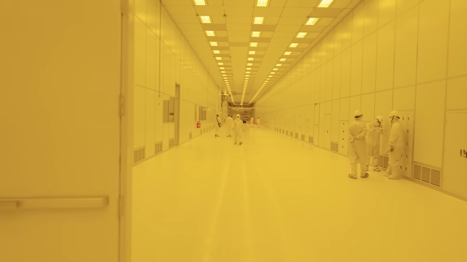
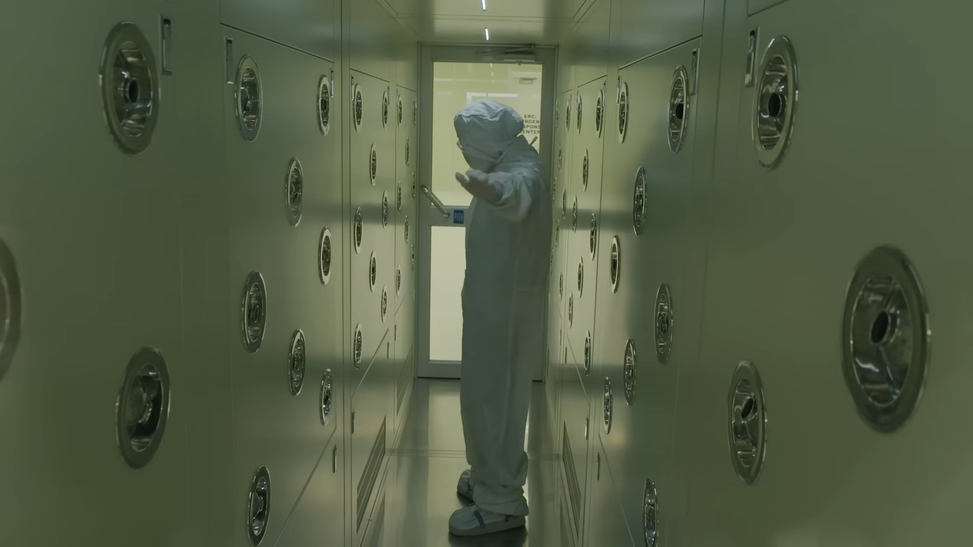
Beyond the astonishing scale, what's most impressive is just how much of the facility—and the tech inside—looks like it comes straight from a science fiction movie. Amid hundreds of workers dressed in "bunny suits" to prevent contamination of the production line, the clean rooms themselves are filled with robotic modules traversing the ceilings on railway-like lines above, referred to as "the silver highway".
The Automated Material Handling System looks more advanced than any I've seen before, ferrying wafers around the vast facility in a way that makes you wonder whether any human interaction is needed at all. More impressive still is a CG-recreation of what happens within the ASML lithography machine, and the description of its process.
"In each one of these machines, there is a lot of hi-tech going on," says department manager Konstantinos Ninios. "Plasma ignites. Molecules and atoms move around… one transistor is 10 to 20 thousand times smaller than a human hair."
Scale that up to billions of transistors on a single chip, and the technological achievement of what TSMC is producing is nothing short of astounding. I write about this sort of thing for a living, but nothing brings the sheer scale and complexity home more than seeing the fab operate for yourself, even if computer graphics are relied on for some of the production processes themselves.
What, did you think they'd stick the world's smallest, light-shielded camera in there? We can only hope and dream. One day, perhaps.
A brief note is also made to the vast water requirements of this huge facility, situated in what's estimated to be one of the driest areas in the US. "We think about water on a daily basis," says Chris Camacho, former president and CEO of the Greater Phoenix Economic Council. "We're very aware of the changes related to climate, which affects water and scarcity management."
"Our industrial reclamation water plant will enable us to recycle and reclaim 90% of the water we use here," continues program manager Lacey Suastegui. Impressive claims, no doubt, although likely a direct response to criticism from local environmental and labor groups regarding the perceived lack of oversight and thorough reviews of the impact of the fab on the state's water supply overall. The water plant is said to still be in the process of construction, whereas the fab itself began producing 4nm chips in January of this year.
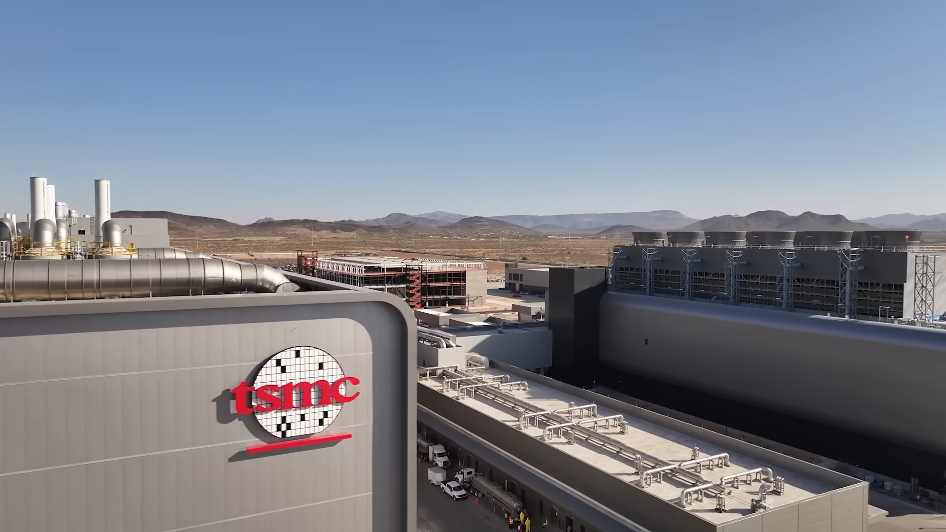
Still, the facility itself is undoubtedly impressive. TSMC is estimated to be responsible for the production of over 90% of the world's most advanced chips, and its Arizona fab (along with a smaller fab in Camas, Washington) represent the first steps towards a larger planned expansion into US chipmaking facilities.
This is eventually expected to result in the construction of three additional fabrication plants, two advanced packaging facilities, and a new development center on US soil—all as part of a new $100 billion investment package, on top of the $65 billion already invested in its Arizona facility.
So, next time you boot up your gaming PC, it's worth taking an extra-long stare at the components ticking away inside. Many of those chips came from mega-expensive, sci-fi-like facilities like this one, and you're using them to play games, check your social media, and fall into ever-increasingly deep rabbit holes on YouTube. It's the circle of tech, right there. Ain't it beautiful?


 Bengali (Bangladesh) ·
  English (United States) ·